
info@kosartech.com
Author: Ali Kosari Mehr
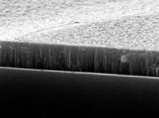
In 2003, the influence of substrate bias voltage and the ratios of nitrogen flow rate to argon flow rate was investigated on the crystalline structure of Cu3N films. For the films deposited in a sufficiently low nitrogen flow rate (e.g., 2 smL min-1), the (100) and (111) planes of Cu3N are detected in the XRD patterns with no substrate bias voltage being applied. However, as the bias voltage increases, the intensity of the peaks corresponding to these planes decreases until being equal to zero, and the peaks corresponding to the (100) and (111) planes of Cu emerge. For the films deposited in a sufficiently higher nitrogen flow rate (e.g., 4, 7, and 10 smL min-1), the peaks corresponding to the planes of Cu3N and Cu are both observed in the XRD patterns with the bias voltage being applied; the increase in the value of bias voltage leading to the decreased intensity of Cu3N peaks and the increased intensity of Cu peaks [1]. Furthermore, in a recent study, the crystalline structure of Cu3N films deposited in a pure nitrogen atmosphere was studied with various bias voltage being applied to the substrate. And, it was revealed that no peaks corresponding to the Cu planes are observed in the XRD patterns, with/without the bias voltage being applied [2].
With regard to what was mentioned, it can be seen that the XRD patterns of the deposited copper nitride films – inclined to lose nitrogen as it is subjected to ion bombardment – show Cu phase as well by applying bias voltage to the substrate – owing to the nitrogen re-sputtering effect. Moreover, it could be asserted that substrate bias voltage and nitrogen-argon flow ratio exert opposite effects on copper (Cu)/copper nitride (Cu3N) phase in XRD patterns of Cu3N films. In other words, at higher ratios of nitrogen flow rate to argon flow rate, a higher substrate bias voltage is required to eliminate the Cu3N phase in the XRD patterns [1,2].
1. Pierson JF (2003) Influence of bias voltage on copper nitride films deposited by reactive sputtering. Surf Eng 19:67–69. Webpage
2. Zamani Meymian MR, Delavari Heravi A, Kosari Mehr A (2020) Influence of bias voltage on optical and structural characteristics of Cu3N films deposited by reactive RF magnetron sputtering in a pure nitrogen atmosphere. Mater Sci Semicond Process 112:104995. Webpage
3. Zhang G, Lu Z, Pu J, et al (2013) Structure and Thermal Stability of Copper Nitride Thin Films. Indian J Mater Sci 2013:1–6. Webpage

