
info@kosartech.com
Author: Ali Kosari Mehr
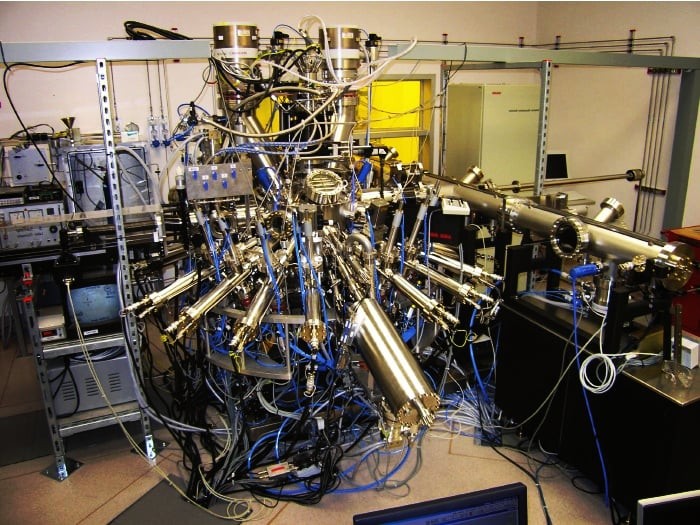
Molecular beam epitaxy (MBE) is one of the most reliable thin-film deposition methods based on thermal evaporation. Equipped with a computerized process control unit, this controllable system can control the evaporation rate of materials in the source. In this regard, a typical MBE system is comprised of a growth chamber, an analysis chamber, and a sample chamber. Nowadays, this technique is widely deployed for the controlled deposition of compounds and alloys. For instance, superlattice structures of GaAs/GaAlAs can be obtained by the technique.
Various factors should be considered in an MBE process, amongst which the presence of the ultra-high vacuum (i.e., the pressures of residual gases lower than 10−7 Pa) in the vicinity of the effusion cells (i.e., crucibles consisting of source material and a heating source) and the substrate is of immense significance for the deposition of high-quality materials. However, it is noteworthy that the residual gas pressure required for the deposition of high-purity Si or GaAs is fairly lower than the pressure typical of ultra-high vacuum (lower than 10−9 Pa). Hence, in the MBE systems, the vacuum bake-out process (i.e., the process of utilizing heat and vacuum for eliminating volatile compounds from objects) and a titanium sublimation pump (the process of utilizing titanium atoms, very reactive, for reacting with residual gas in ultra-high vacuum systems) are usually utilized.
As mentioned before, an MBE system is comprised of three chambers: The substrate is placed in the first chamber in order that degasification of the substrate can occur. The second chamber called the analysis chamber is the place where analysis tools (e.g., Auger electron spectroscopy and X-ray photoelectron spectroscopy) are installed. The role of the second chamber is also to be a buffer between the first and third chambers in order to prevent the external impurities from entering the third chamber. The third chamber is the place where the deposition process is carried out.

